Nanoscale
-
 It's long been assumed that when a metal structure like a bridge or an engine develops a crack, it will only get worse over time. But that might not be the case, based on what researchers have just observed happening in a piece of platinum.
 -
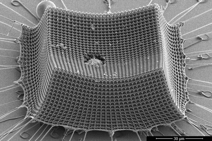 A light weight and slim form are two very desirable attributes when it comes to next-gen armor materials. With this in mind, scientists have used advanced nanoscale engineering to craft a new armor material they say outperforms Kevlar and steel.
 -
 Researchers at Empa and EPFL have created one of the smallest motors ever made. It’s composed of just 16 atoms, and at that tiny size it seems to function right on the boundary between classical physics and the spooky quantum realm.
 -
 It sounds like a scene from Ant-Man, but this is very much real life: scientists at MIT have devised a super shrinking system that can produce 3D nanoscale versions of much larger, custom-made objects – reducing them to around one thousandth the size of the originals.
 -
 MIT engineers recently managed to create cell-sized robots that could collect data about their environment, but were a little tricky to manufacture. Now, the team has found a way to mass produce these synthetic cells (syncells) through controlled fracturing of graphene.
 -
 A new technique developed at Berkeley Lab allows liquid 3D structures to be printed within other liquids. This new form of 3D printing could give rise to flexible and stretchable liquid electronics, aid chemical synthesis, or serve as a transport and delivery system for nanoscale particles.
 -
 Researchers at the Queensland University of Technology (QUT) have used a new technique to produce detailed images of dragonfly wings, showing more than 10 billion tiny 'fingers' (nanostructures) lining the wing surface that make bacteria tear themselves apart.
 -
 Generally, water repellent objects and those that attract or absorb water have very different microscopic-level attributes. Now researchers have discovered a way to use a single type of material to perform both functions, switching between the two simply by applying electric current.
 -
 A nano-scale engine made from tiny charged particles of gold has just been declared the world's smallest by researchers at the University of Cambridge who created it.
 -
 A team of physicists have just created the world's smallest working engine from a single electrically-charged atom. With an equivalent efficiency (if scaled to size) of an average automobile engine, it actually produces a significant amount of power
 -
 A team of engineers has created a steel alloy that is much stronger than ordinary steel and is so resilient that it bounces back into shape, even when blasted with a cannon. The researchers believe it could make super-strong armor or help protect space vehicles from micrometeorites.
 -
 A versatile origami fold could be the key to creating just about any structure, from the nanoscale to full-scale buildings, according to new engineering research out this week. A team at Harvard says the key is a folding pattern known as the Miura-ori.
Load More