Stanford engineers have pioneered a new design for a scalable 3D computer chip that tightly interconnects logic and memory, with the effect of minimizing data bottlenecks and saving on energy usage. With further work, the advance could be the key to a very substantial jump in performance, efficiency, and the ability to quickly process very large amounts of information – known as "Big Data" – over conventional chips.
Bottlenecks
A chain is only as strong as its weakest link. In the context of chip design, that link is usually the data bus that connects the memory and logic components and fetches data from memory, delivers it to the logic units for processing, and then sends it back over for storage.
As it turns out, both CPU speeds and memory size are advancing at a much faster rate than the throughput speed of the data bus is improving. This means that when processing large amounts of data the CPU has to slow down to a crawl, constantly waiting for new data to arrive, wasting a lot of time and energy in the process. And things are only going to get worse as the gap increases. Couple this trend with the huge interest in Big Data in recent years and it’s easy to see how, if nothing is done to address this, we might end up with a serious problem on our hands.
One way to deal with the data bottleneck could be to ferry data inside a chip using the much faster optical fibers, though the technology still seems quite far from mass production. Instead, a team led by professors Subhasish Mitra and Philip Wong at Stanford is exploring the more radical avenue of creating dense 3D chips that integrate memory and logic right on top of each other, and that exchange data using an array of thousands of vertical nanoscale interconnections. The sheer number of short-distance connections allow the data to travel much faster, using less electricity, and sidestepping the bottleneck problem almost entirely.

"The memory is now right on top of the logic, so the data doesn’t have to move back and forth across long distances," lead author of the paper Max Shulaker tells Gizmag. "Putting them so close together (vertically over one another) therefore saves a lot of energy in passing data back and forth between the logic and memory. Also, now that the bandwidth between the memory and logic is greatly increased, the processor doesn’t have to waste time or energy waiting to get the data."
A prototype 3D chip built by the researchers packs four layers on top of each other, two layers of memory "sandwiched" between two layers of logic. This shows that the researchers are able to stack all possible combinations on top of each other – memory on logic, memory on memory, logic on memory, and logic over logic. "But you could build even more layers using the exact same methodology depending on what your application required," says Shulaker.
A matter of temperature
This sort of close-quarters stacking is not possible in your standard chip because manufacturing a memory chip requires very high temperatures, on the order of 1,000° C (1,800° F), which would melt down the layer below it.
So the team opted for a special type of memory which they had previously developed, called RRAM (for "resistive random access memory"). It doesn’t use silicon, but rather a combination of titanium nitride, hafnium oxide and platinum. Applying electricity to the memory cell one way causes it to resist the flow of electricity (hence the name), which equates to a "0" bit, while applying voltage the opposite way causes the structure to conduct again – representing a "1" bit.
Apart from consuming less energy, the advantage of RRAM is that it can be built at much lower temperatures, meaning it can be manufactured right on top of other circuits, paving the way for building functional 3D chips.
Interestingly, the transistors which are part of the "high-rise" design can be either standard silicon field-effect transistors (Si-FET) or made out of the much more energy-efficient carbon nanotubes (CNFET). In a previous study, Mitra, Wong and colleagues found a way to manufacture what they say are some of the highest-performing nanotube-based transistors to date.
"We benchmarked our CNFETs against silicon-based transistors which are in production today," Shulaker tells us. "We take the foundry models (the models the companies that make the silicon transistors use) for the silicon transistors, and change parameters in their models to match the CNT transistors we make in our lab at Stanford (since industry labs can print much smaller transistors than we can in an academic lab), and we see that our CNT transistors are now competitive with these silicon transistors."
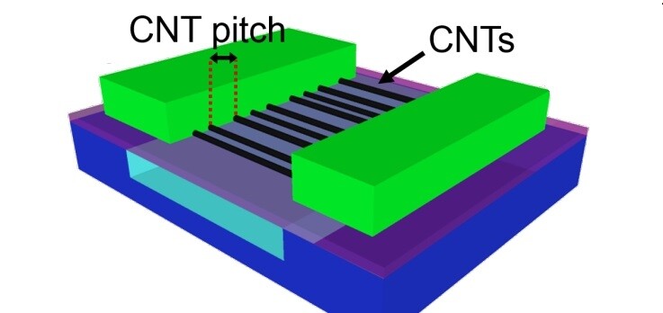
Previous CNTFETs could not reach high levels of performance because the concentration of carbon nanotubes was too low to build an effective chip. The Stanford team used a simple but ingenious workaround: the researchers started growing the nanotubes as usual and then used a sort of metal "Scotch tape" to transfer the nanotubes onto a silicon wafer that would serve as the base of the chip. Repeating the process 13 times per wafer resulted in a very high-density carbon nanotube grid.
"It is projected that CNT transistors will achieve an order of magnitude benefit in energy-delay product – a metric of energy efficiency – compared to silicon CMOS once we can work out the remaining obstacles," Shulaker continues. "Thus, for one third the amount of energy, your circuit would run three times faster, for instance."
Interconnections
As the scientists deposited each memory layer, they were also able to create thousands of nanoscale interconnections into the logic layer below, which are meant to serve the role of the data bus. The great number of connections, along with the extremely short distances that data has to travel, allows the chip to avoid the data "traffic jams" that are plaguing current chip designers.

As you can see from the figure above, the interconnections between the logic and memory can be arbitrary. In the first layer from the bottom, the logic layer is made out of standard (Si-FET) transistors, demonstrating how this design can integrate with existing technology.
Crunching Big Data
This research is still in its early stages, but the scientists say their design and manufacturing techniques are scalable and could lead to a significant leap in computing performance.
"Monolithic 3D integration of logic and memory and emerging nanotechnologies like CNT transistors are promising steps for building the next generation of ultra-high efficiency and high performance electronic systems that can operate on massive amounts of data," says Shulaker. "The ability to operate on massive amounts of data in an energy-efficient manner could enable new applications that we can’t dream of today."
The next step for the team will be to use this integration scheme to demonstrate new systems that cannot be built using today’s technologies and which leverage the data-crunching abilities of such systems.
"Paradigm shift is an overused concept, but here it is appropriate," says Prof. Wong. "With this new architecture, electronics manufacturers could put the power of a supercomputer in your hand."
Two papers describing their advance were presented at the IEEE International Electron Devices Meeting (IEDM) on December 15–17.
Source: Stanford University