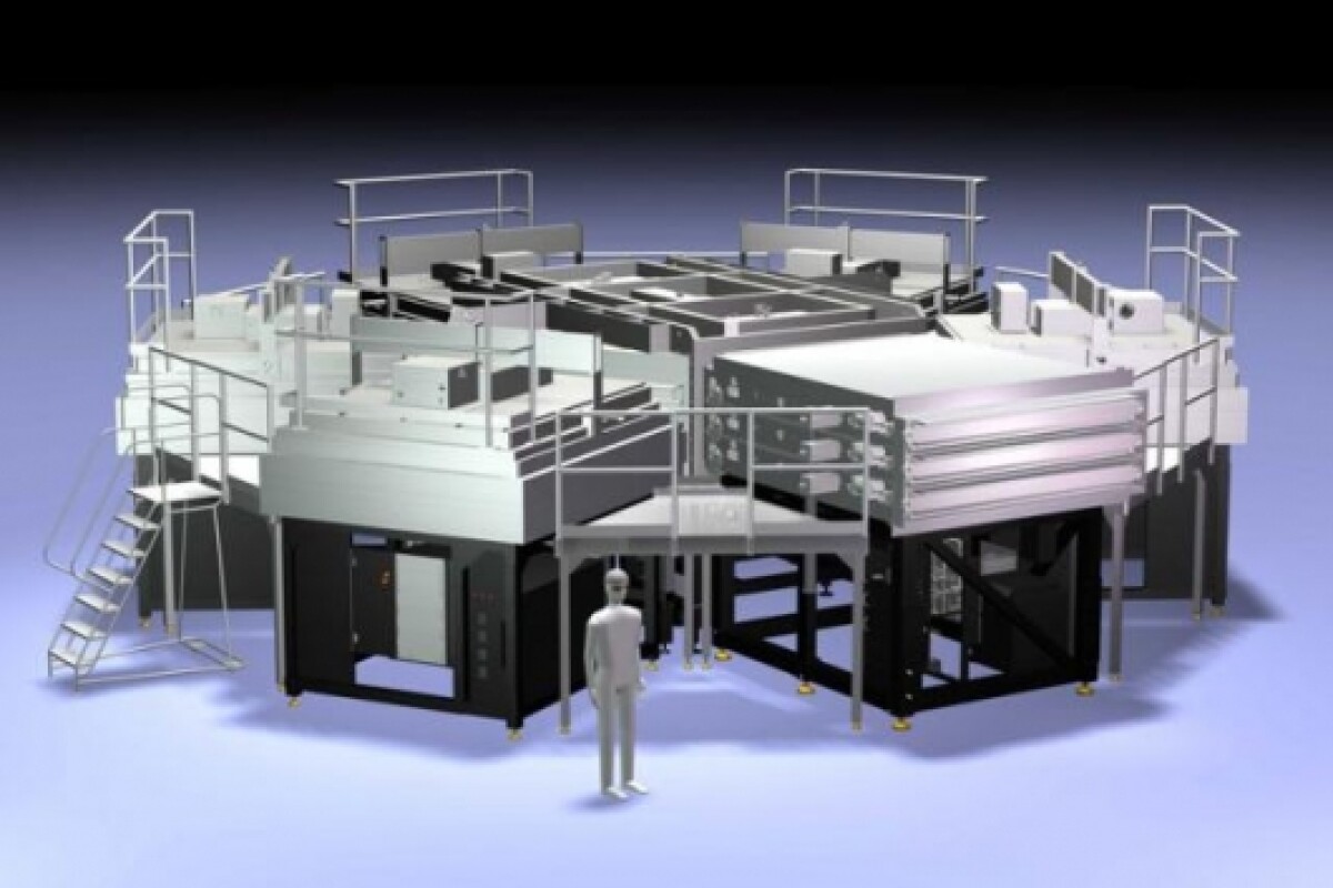


October 18, 2006 Ever wondered what a machine that produces flat panels looks like – well wonder no more – this little baby is a new breed of highly-efficient machine that enables the production of six 55inch LCD TV screens from Gen 8.5 (2.2m x ~2.5m) glass substrates at a time. Applied Materials provides Nanomanufacturing Technology solutions for the electronics industry and has produced it as the first of several suites designed to reduce the total cost of flat panel manufacturing. The new Gen 8.5 panels are expected to contribute to TFT-LCD TV market growth, which is forecast by market researcher Display Search to exceed 40 million units in 2006.
“Applied Materials continues to help customers reduce the total cost of flat panel manufacturing by providing differentiated products and technologies supported by its worldwide service capabilities,” said Dr. Mark Pinto, senior vice president and general manager of Applied Materials’ New Business and New Products Group and AKT.
“Applied has steadily increased its position in FPD equipment, beginning with PECVD technology for transistor formation, then adding e-beam test, and now addressing sputtered films in the color filter area. By combining our leadership in large area processing with our strengths in Nanomanufacturing Technology, this new suite of products puts us at the forefront of the display equipment business and gives our customers a highly productive, cost-effective and reliable set of technologies for next generation manufacturing.”
The AKT-55K EBT system features one of the industry’s fastest and most accurate pixel test technology with the lowest overall operating costs. The system features seven electron beams to provide rapid, accurate pixel array testing. The system’s non-contact test technology ensures safe testing of high-value LCD TV panels without damaging or scratching the display.
The AKT-55K PECVD system utilizes the proven multi-chamber platform architecture and technology that have made AKT the industry leader in flat panel CVD equipment for the past 13 years. Optimized for both dielectric films (SiNx, SiOx and SiON) and semiconducting films (a-Si and doped a-Si), the AKT-55K system can process over 60 substrates per hour for single-layer films.
For color filter manufacturing, the AKT-NEW ARISTO 2200 is a fully-automated vertical sputter system optimized for high productivity and target utilization. Based on the market-leading NEW ARISTO system concept, formerly from Applied Films, the AKT-NEW ARISTO 2200 uses an innovative planar cathode design optimized for low defects and high yield, while providing the highest throughput in the industry.
(1) LCD: liquid crystal display; PECVD: plasma enhanced chemical vapor deposition; TFT: thin film transistorContacts