Science

Building circuit boards using DNA scaffolding

Building circuit boards using DNA scaffolding
High concentrations of triangular DNA origami binding to wide lines on a lithographically patterned surface; the inset shows individual origami structures at high resolution
View 9 Images
1/9
2/9
3/9
High concentrations of triangular DNA origami binding to wide lines on a lithographically patterned surface; the inset shows individual origami structures at high resolution
4/9
High concentrations of triangular DNA origami binding to wide lines on a lithographically patterned surface; the inset shows individual origami structures at high resolution
Individual triangular DNA origami adhering to a template with properly sized triangular features
5/9
Individual triangular DNA origami adhering to a template with properly sized triangular features
Low concentrations of triangular DNA origami binding to wide lines on a lithographically patterned surface
6/9
Low concentrations of triangular DNA origami binding to wide lines on a lithographically patterned surface
7/9
8/9
9/9
View gallery - 9 images

There have been a few breakthroughs in recent years that hold the promise of sustaining Moore’s Law for some time to come. These include attaching molecules to silicon and replacing copper interconnects with graphene. Now IBM are proposing a new way to pack more power and speed into computer chips by using DNA molecules as scaffolding for transistors fabricated with carbon nanotubes and silicon wires.

The new approach developed by scientists at IBM and the California Institute of Technology uses DNA molecules as scaffolding or miniature circuit boards for the precise assembly of components such as millions of carbon nanotubes, nanowires and nanoparticles, that could be deposited and self-assembled into precise patterns by sticking to the DNA molecules.

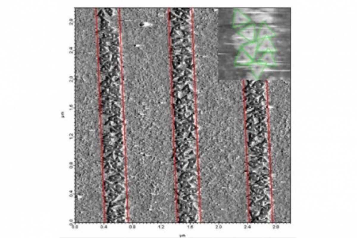
The researchers say such a technique may provide a way to reach sub-22 nm lithography on surfaces compatible with today’s semiconductor manufacturing equipment. The technique allows for DNA nanostructures such as squares, triangles and stars to be prepared with dimensions of 100-150 nm on an edge and a thickness of the width of the DNA double helix.

“The cost involved in shrinking features to improve performance is a limiting factor in keeping pace with Moore’s Law and a concern across the semiconductor industry,” said IBM researcher, Spike Narayan. “The combination of this directed self-assembly with today’s fabrication technology eventually could lead to substantial savings in the most expensive and challenging part of the chip-making process.”

The research is detailed in the paper, “Placement and orientation of DNA nanostructures on lithographically patterned surfaces,” will be published in the September issue of Nature Nanotechnology.

View gallery - 9 images
1 comment
1 comment
waltinseattle
can't wait to read ALL about it when the paper is published. Thanks for the advance publicity.
I always wonder how they expect to insure reliability as the size and energy levels deminish to random fluctuations of the field. Can these wonders only run behind the world's most exact farady shielding? or can I use the tech on the street with RF and cosmic noise?
On an entirely different side of reacting: what does this say about the nature of life, sentience and the posibility of most unusual, even "alien" life forms? i.e. that colliny as a computing storing sentient being, not just a mass in a petri dish?