Materials

Graphene takes on a new dimension

Graphene takes on a new dimension
A new process for creating 3D objects out of graphene opens up the possibility of fashioning a whole new range of innovative electronic devices (Credit: Shutterstock)
View 2 Images
Researchers have discovered a way to produce three-dimensional shapes in graphene, which may lead to a range of superior graphene components being developed to replace standard silicon devices
1/2
Researchers have discovered a way to produce three-dimensional shapes in graphene, which may lead to a range of superior graphene components being developed to replace standard silicon devices
A new process for creating 3D objects out of graphene opens up the possibility of fashioning a whole new range of innovative electronic devices (Credit: Shutterstock)
2/2
A new process for creating 3D objects out of graphene opens up the possibility of fashioning a whole new range of innovative electronic devices (Credit: Shutterstock)

Graphene is themodern go-to material for scientists and engineers looking to create all manner of new electronic devices. From ultra-frugal light bulbs (bothbig and small), to super-efficient solar cells, flexible displays and much more, graphene is a multi-tasking marvel. However, in all ofthese instances, graphene in its original form of atom-thin, flat sheets has had to be used with peripheral supports and structures because it lacks a solid shape and form of its own. Now researchers from theUniversity of Illinois at Urbana-Champaign (UIUC) have come up with a way of creating3D objects out of graphene that opens up the possibility of fashioning a whole new range of innovative electronic devices.

To create 3D shapes in graphene, the researchers first had to ensure that their approach was sufficient to maintain the structural integrity of the material when it was subjected to deformation. As such, the team used an underlying substrate former over which they laid a film of graphene that had been soaked in solvent to make it swell and become malleable. Once overlaid on the former, the solvent then evaporated over time, leaving behind a layer of graphene that had taken on the shape of the underlying structure. In this way the team was able to produce a range of relatively intricate shapes.

Researchers have discovered a way to produce three-dimensional shapes in graphene, which may lead to a range of superior graphene components being developed to replace standard silicon devices

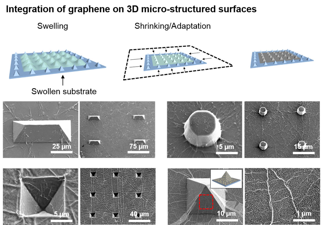
"To the best of our knowledge, this study is the first to demonstrate graphene integration to a variety of different microstructured geometries, including pyramids, pillars, domes, inverted pyramids, and the 3D integration of gold nanoparticles (AuNPs)/graphene hybrid structures," said SungWoo Nam, assistant professor of mechanical science and engineering at UIUC. "Our swelling, shrinking, and adaptation steps are optimized to minimize the degree of graphene suspension around the 3D microstructures and facilitate successful 3D integration. We control the amount of substrate swelling by adjusting the time of immersion in organic solvent and the mixing ratios of monomer and curing agent of the polydimethylsiloxane (PDMS) substrate."

Varying in size from just 3.5 to 50 μm, the dimensions of the graphene microstructures developed by UIUC put them right in the middle of a range of electronic devices, including various types of photodetectors, nano antennas, and other sub-miniature components that were once only the domain of silicon-based products. According to the team, these factors, along with graphene's high carrier mobility, chemical inertness, and biocompatibility, mean that three-dimensional graphene could be adapted over even wider areas.

"We also expect that our new 3D integration approach will facilitate advanced classes of hybrid devices between microelectromechanical systems (MEMS) and 2D materials for sensing and actuation," said SungWoo Nam.

Due to the fragility of atom-thin graphene, previous methods to bend or mold it into complex shapes resulted in uneven, ill-formed objects at best, and a ruptured mess at worst. In investigating the new technique, the researchers at UIUC were diligent in their testing of the formed graphene via electron microscopy, atomic force microscopy, Raman spectroscopy, and electrical resistance measurement to confirm that it maintained its shape and consistency after forming.

"Our results demonstrate a simple, versatile, and scalable method to integrate graphene with 3D geometries with various morphologies and dimensions," said Jonghyun Choi, a graduate student in Nam’s research group. "Not only are these 3D features larger than those reported in previous works, but we also demonstrate the uniformity and damage-free nature of integrated graphene around the 3D features."

The results of this research were recently published in the journal Nano Letters.

Source: University of Illinois at Urbana-Champaign

5 comments
5 comments
S Michael
You know... people have been touting this stuff now for years. Graphene, Graphene, Graphene. BUT nobody has come up with a way to produce this stuff in large enough quantity to put it on the market..
Geez.... stop talking and make it happen. If you can't then move on. Tired of hearing about all the wonderful things it could do, but never seems to make it to market where it counts.
Kevin Ritchey
Sounds like this has applications in a multitude of areas but I want to see research directed towards the battery market. So many new devices are relying on the same old technology that has been around since the Bagdad battery was discovered.
attoman
Shrinkage and other factors visible in the SEM images suggest that the film is neither single monolayer nor without extensive faults.
Experiments demonstrating the strength and integrity of the film formed over 3D structures is entirely necessary before any reasonable projection of utility for this method.
Perhaps the paper has evaluated the integrity of the 3D structures. Unfortunately the paper is locked behind a high dollar wall. So its incumbent that the author of this piece answer the question or attach the pertinent part of the article in Nano Letters.
rodr48
Graphine was going to be the new space age material that aircraft would be made of, cars, etc, etc but nothing has happened. A cure for cancer is found every week as well??, cars will run on sola/hydrogen and cost nothing to run......... all a little hard to father.....mi no savy...RR
DG
There is continuing developments sort of a race to low cost energy in vast quantities.
The computers around the world keep using more and many of our home uses continue to increase.
The on going changes is increasing and similar to the increase in power of the home computer is increasing at a higher and higher rate compounded.
Society will change or get left behind in the technology.
Those societies that accept and use the new technology innovations will grow and the others will be left in the past as well as being left in the dust of bye gone technology.
USA is moving very fast into the Era of Knowledge and applied technology.
Take this in stride and learn to embrace this new technology and reduce the labor and increase your independence.
I do believe the super capacitors may replace the ion battery and increase the range of electric cars.
The gas an diesel power generation will be phased out over many many years.
Change over from high energy light bulbs will move to LEDS and if you change over on those used the most you eventually get change over to the lowest cost of use but a higher cost of buying these new devices.
Welcome to the brave new world.