Photography
News, reviews of the latest cameras, and image galleries featuring the work of the world's best photographers.
Latest News
-
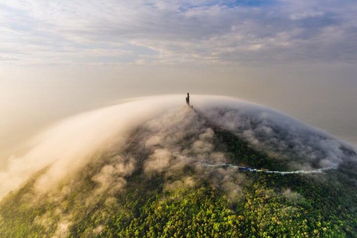
Sony World Photography Awards showcases beauty of the natural world
April 19, 2024The overall winners of the 2024 Sony World Photography Awards have been revealed. This year's selection of images showcases a sublime mixture of unspoiled landscapes, amazing animals, and extraordinary people going about their lives. -

Mirrorless goes micro with pocket-friendly travel camera
March 28, 2024Colorful photo-tech inventor Samuel Mello Medeiros and camera/optics veteran Yashica have joined forces to create what's billed as the world's smallest mirrorless camera, the Micro Mirrorless Yashica – I'm Back. -

Coalax Lancer 300 modular backpack may just be the Robocop of camera bags
March 26, 2024The Coalax Lancer 300 modular photography backpack is very much a modern-day descendant of the humble camera bag. Among other things, it sports a removable power bank, solar panel, drone-carrying compartment, and extendable rotatable selfie sticks. -
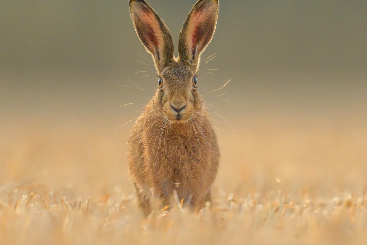
Hare for it: 2024 British Wildlife Photographer of the Year winners
March 14, 2024A dramatic image of a soccer ball covered in invasive goose barnacles has taken out the top prize in this year's prestigious British Wildlife Photography Awards, beating out more than 14,000 entries that aimed to cleverly capture the world around us. -

Swift-Lock system brings quick-release pizzazz to camera straps
March 06, 2024Carrying your camera could soon get a lot easier. The Swift-Lock system allows users to tote their DSLR in a stabler, more accessible orientation than otherwise, plus they can quickly pop their camera on and off of the thing as needed. -

MicroBOOM lets solo videographers shoot boom-mic'd interviews
February 08, 2024Boom mics are great for shooting interviews on the go, but they have to be held by a sound person who stands beside the videographer. The MicroBOOM pole is different in that it mounts right to the camera, allowing one person to do everything. -

Motorized, self-leveling tripod takes the strain out of video shoot setup
February 02, 2024Photo and video gear company Edelkrone teased its "biggest launch in years" in October last year, and has now revealed all with the release of the "world's first" fully motorized, self-leveling tripod called the X. -

OM Systems OM-1 flagship 4/3 camera first to feature Live Graduated ND
January 30, 2024Back in 2022, OM Digital Systems celebrated the 50th birthday of the Olympus OM-1 film camera with a digital four-thirds model. Now the OM System flagship has moved to its second generation, though despite key updates much remains the same. -

Hasselblad launches fast-focus 100-MP medium-format camera system
January 24, 2024Imaging titan Hasselblad has announced the successor to 2020's 50-megapixel 907X 50C digital camera system. The 907X & CFV 100C model boasts a camera back featuring a 100-MP back-illuminated image sensor that can be used with legacy film cameras. -
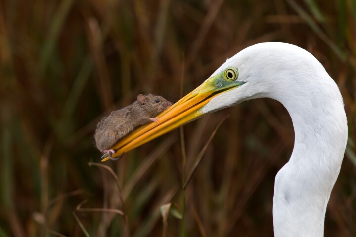
Shy sea lion and orangutan operation lead Nature Photo Contest wins
January 16, 2024A new photography competition has released its first batch of winners and finalists. A portrait of a playful sea lion has won the inaugural Nature Photography Contest, which showcases animals, plants, landscapes and human impact on the environment. -

"Millennium Camera" to take a 1,000-year long-exposure photo
January 09, 2024What did your area look like 1,000 years ago? Well, people in the year 3023 might have the luxury of finding out, thanks to an art/science project called the Millennium Camera, which will take an extremely long-exposure photo of the Arizona desert. -

Universal Lite turns almost any smartphone into an underwater camera
January 09, 2024Although most smartphones are now waterproof, you definitely shouldn't take them snorkeling without an underwater housing. The Universal Lite is one such device that fits a wide range of phones, allowing them to serve as underwater cameras. -
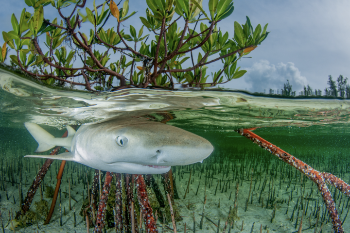
Best photos of 2023: Animals, aurorae and amazing landscapes
December 27, 2023Every year, countless stunning images are submitted to photography competitions around the world. From cosmic structures to microscopic marvels and everything in between, here is a snapshot of the most awe-inspiring photographs of 2023. -

Gallery of Fluid Motion: Science at its most visually stunning
December 18, 2023In fluid dynamics, hard science often comes with dazzling aesthetic beauty – a fact the American Physical Society highlights annually with a photo/video contest. Here are this year's winners – equal parts fascinating, hypnotic and visually stunning. -
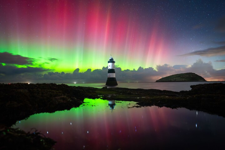
Powerful solar storms dazzle in annual aurora photography gallery
December 05, 2023In good news for aurora photographers, the Sun is approaching the most active period of the solar cycle. As such, the stunning light shows in the 2023 Northern Lights Photographer of the Year collection are particularly vibrant.
Load More