Nanowires
-
 Ice build-up can pose a problem for roads, aircraft, wind turbines and power lines, among many other things. Now scientists have developed a new structure made of copper nanowires that can passively de-ice surfaces with an efficacy of close to 100%.
 -
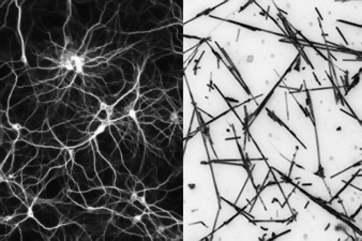 Nanowire networks mimic the networked structure of the human brain. But can they learn and remember like a human brain can? New research indicates they can.
 -
 Motion-measuring strain sensors have many uses, such as tracking a person's physical activity, or reading their blood pressure. A new such device could be particularly useful, as it combines high sensitivity with a wide range of detectable motion.
 -
 Copper is known for its ability to kill microbes on contact, which is why it's often professionally coated onto commonly touched items. A copper nanowire spray may allow everyday folks to give existing surfaces the same treatment, using a spray can.
 -
 Heat is a major hurdle for electronic devices. Scientists have now found that nanowires made of a certain isotope of silicon can conduct heat 150 percent better than regular silicon, potentially leading to drastically cooler computer chips.
 -
 Engineers from North Carolina State University have developed a thin, stretchable electronic wearable sleeve that allows the user's skin to breathe, making for more comfortable long-term use as a biomedical sensor or human-machine interface.
 -
 We've already heard about so-called "fog harps" that use thin wires to collect airborne water droplets, providing drinking water. Well, an experimental new device also uses wires to capture water vapor, although it proceeds to generate electricity.
 -
 Scientists are coming up with some creative new methods to fight cancer. Now, a new study has found that iron nanowires could deliver a three-pronged attack against cancer cells, using heat, vibrations and drugs together.
 -
 Metamaterials that cloak people and objects from radar, visible light or infrared are usually thick and heavy, but now engineers at the University of Wisconsin-Madison have developed an ultrathin, lightweight sheet that absorbs heat signatures and can even present false ones.
 -
 ScienceIt's never a good thing when donated human blood – or even the blood in our bodies – is infected with bacteria. Scientists at the University of California San Diego, however, are developing a means of removing such blood-borne microbes using tiny ultrasound-powered robots.
 -
 Researchers have broken the efficiency record for nuclear fusion on the micro-scale. Using an ultra-fast, high-powered laser, the results were about 500 times more efficient than previous experiments. The researchers blasted arrays of nanowires to create incredibly hot, dense plasmas.
 -
 Smartphone screens seem to crack at the slightest breeze, but researchers at the University of Sussex might have a hardier alternative. A new material made of graphene and silver could lead to touchscreens that are tougher, easy to manufacture, more responsive, less power-hungry, and even bend.
Load More