
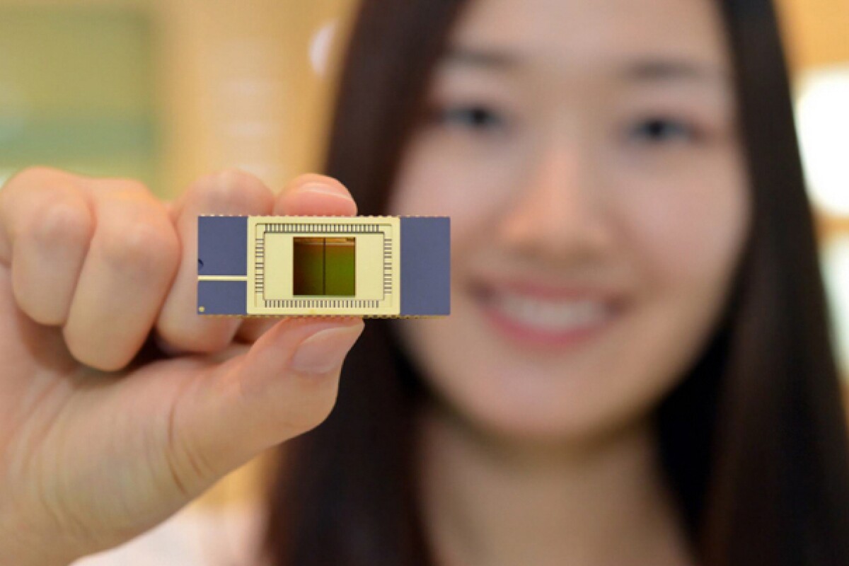


Samsung has announced production of the first solid state drives (SSD) based on its new 3D V-NAND flash memory. V-NAND flash memories read and write twice as fast as conventional NAND memories, and last 10 times longer while consuming 50 percent less power. At present, the 3D chips offer about the same physical bit density as do more conventional NAND flash memory chips, but while 2D geometries are reaching the end state of their scaling potential, the 3D chips offer as much as two orders of magnitude of additional elbow room for denser devices.
Flash memory has been one of the miracle stories of the 21st century. Invented in 1980, flash memory drives hit the market in the mid-1990s with a storage capacity of 2 MB. Flash memory has been following or exceeding Moore's law for some time and 20 years on, capacity has increased to over 64K times the original figure.
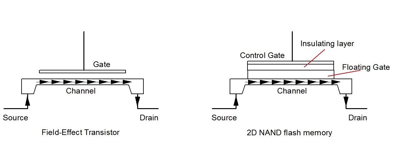
The newest flash chips are made using 10-nm lithography, and are starting to run into physics-based problems. A NAND flash memory is a floating-gate transistor, in which an isolated gate layer can store charge for long periods of time. The memory is read by measuring the conductivity of the device channel as the control gate is pulsed. The memory cell gives a response if there is no stored charge, and no response if there is stored charge, thereby allowing non-destructive reading of the memory.
At least two sources of difficulty are appearing as a result of fabricating NAND flash memory in smaller sizes. First, each gate only holds a handful of electrons, so that small imperfections lead to memory states that are difficult to differentiate. Second, the control electrodes are so small and so closely spaced that their effects spread over more than one memory cell, leading eventually to unreliable reading and writing of data.
The 3D V-NAND flash geometry compensates for this problem by finding more room to move in the vertical direction. The first change is to a charge trap flash geometry, pioneered in 2002 by AMD. In a charge trap flash memory cell, the stored charge is not located on a floating gate, but rather on an embedded silicon nitride film. Such a film is more robust against point defects which form in the heavily-doped polycrystalline silicon making up a typical floating gate. It can also be made thicker, to hold larger numbers of electrons making the cells less sensitive to electron loss.

The second change is to wrap a planar charge trap cell into a cylindrical form. As shown in the figure above, growth of a group of V-NAND cells (in this case, a vertical stack of eight cells) begins with forming an alternating stack of conducting (doped) polysilicon layers (in red) and insulating silicon dioxide layers (in blue).
The next step is to etch or otherwise form a cylindrical hole through these layers. In practice, a 128 Gbit V-NAND chip with 24 layers of memory cells requires formation of about 2.9 billion such holes. Next a conformal layer of silicon dioxide is deposited, which coats the inner surface of the hole, followed by a similar layer of silicon nitride, and a second layer of silicon dioxide. The silicon nitride is the charge-trapping layer, and the silicon dioxide layers for the gate and the tunnel dielectric. Finally, the center of the hole is filled in with conducting (doped) polysilicon that forms the channel of the memory cells.
An individual memory cell (circled on the photo) is made up of one planar polysilicon layer containing a hole whose inner surface acts as the gate electrode, a vertical shell of silicon dioxide as the gate dielectric, a vertical shell of silicon nitride that stores charge, a vertical shell of silicon dioxide as the tunnel dielectric, and a central rod of conducting polysilicon which acts as the conducting channel. Memory cells which are in different vertical layers do not interfere with each other, as the charges cannot move vertically through the silicon nitride storage medium, and the electric fields associated with the gates are closely confined to the vertical layer in which they lay. Finally, the vertical collection of flash memory cells is identical electrically to the serial-linked groups in which conventional NAND flash memory is configured. In the end, the effect of going 3D is to allow larger bit densities without requiring smaller individual memory cells.
Samsung is now supplying samples of V-NAND solid state drives for enterprise applications. Available in 480 and 960 GB capacities, the write speeds are about 20 percent faster than Samsung's earlier SM843T 980 GB SSD, while the power consumption is decreased by about 40 percent. More importantly, the endurance of the 3D drives is about 10 times greater than the SM843T, opening up additional applications that require data juggling on a level that would render last-generation technology SSDs impractical. There's no word yet as to when the new SSDs be available for the rest of us.
Source: Samsung Electronics


