It has been a long-standing dream to fabricate superconducting nano-scale wires for faster, more powerful electronics. However, this has turned out to be very difficult, if not impossible, with conventional superconductors because the minimal size for the sample to be superconducting - known as the coherence length - is large. A group of scientists has now fabricated thin films patterned with large arrays of nanowires and loops that are superconducting when cooled below about 30 kelvin (-243 degrees Celsius). Even more interesting, they found they could change their resistance by applying a magnetic field.
The team of scientists from Bar-Ilan University, Israel, and the U.S. Department of Energy’s (DOE) Brookhaven National Laboratory set out to see if they could achieve superconductivity in a thin film material etched to form a pattern of “wires” - much like the circuits etched into computer chips. The Brookhaven team started by using a precision technique for making superconducting thin films atomic layer by layer. They used a process called molecular beam epitaxy to build a material with alternating layers of copper-oxide and lanthanum and strontium.
Then the team at Bar-Ilan used electron-beam lithography to “etch” a pattern of thousands of loops into the surface of the material. The thickness, or diameter, of the “nanowires” forming the sides of these loops was mere 25 nanometers, while the lengths ranged from 150 to 500 nanometers. Measurements of electrical resistance of the patterned arrays showed that they were indeed superconducting when cooled below about 30 K.
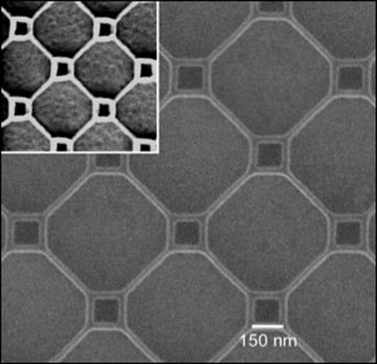
The most widely used superconductor, niobium, has a coherence strength of about 40 nanometers. Very thin nano-wires made of such material wouldn’t act as superconductors. However, in layered copper-oxide superconductors, the coherence length is much smaller - about one or two nanometers within the copper-oxide plane, and as small as a tenth of a nanometer out-of-plane. The fact that these materials operate at warmer temperatures, reducing the need for costly cooling, makes them even more attractive for real-world applications.
When the scientists applied an external magnetic field perpendicular to the loops, they found that the loop resistance did not keep increasing steadily with the field strength, but rather changed up and down in an oscillatory manner.
“These oscillations in resistance have a large amplitude, and their frequency corresponds to discrete units (quanta) of magnetic flux — the measure of the strength of the magnetic field piercing the loops,” said Brookhaven Lab physicist Ivan Bozovic, who synthesized the superconducting films. “A material with such a discrete, switchable form of magneto-resistance — especially from the superconducting to the non-superconducting state — could be extremely useful for engineering new devices.”
The observed frequency of the oscillations in resistance may also have implications for understanding the mechanism by which copper-oxide materials become superconductors in the first place. The current findings seem to rule out certain theoretical models that propose that an ordered alignment of charge carriers known as “stripes” is essential to superconductivity in copper-oxide compounds. A better understanding of the mechanism of superconductivity could lead to even more advances in designing new materials for practical applications.
“Such superconducting nanowires and nano-loops might eventually be useful for new electronic devices - that is the long-term vision,” said Bozovic.
Bozovic and his collaborators describe the research in Nature Nanotechnology.