Computer scientists at MIT have developed a 110-core CPU chip based on a new architecture in which, instead of bringing data across the chip to the core that happens to want it, the program is moved to the core where the data is stored. In practice, this new architecture reduces the amount of on-chip data exchange tenfold, along with cutting the heat and infrastructure demanded by conventional chip architecture.
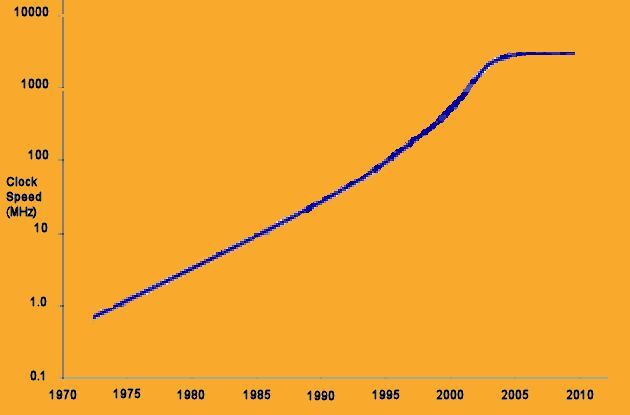
You may have noticed that the rapid progress of computing power has become a bit sluggish in the past decade or so. While Moore's law is still intact, clock speeds have stalled at about 4 GHz, instead of the 50 GHz we would now have achieved based on historical rates of increase.
Multiple-core chips are commonly used to increase peak computing speeds, but run into problems with overheating as data is shuffled back and forth between the cores. MIT professor Srinivas Devadas offers a path to increased computing power by instead moving the program to a core having direct access to the required data.
The number of transistors (MOSFETs – Metal Oxide Silicon Field Effect Transistors) that can be integrated onto a single chip continues to double about every two years, as the feature size of lithographic process technology shrinks. However, Moore's law, as this is called, is only one part of why computing power has grown so rapidly.
The other part is Dennard scaling, which describes how the performance of the MOSFETs scale with decreasing feature size.
MOSFETs
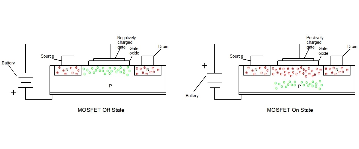
Let's take a quick look at how MOSFETs work. A MOSFET varies the resistance between the n-type silicon source and drain electrodes as the gate voltage changes. In the left-hand figure, a negative voltage is applied to the gate electrode (which is insulated from the rest of the MOSFET by a gate insulator, usually silicon oxide). This negative charge draws the holes (in green) of the p-type silicon closer to the gate. In this configuration, the conduction path through the MOSFET looks like a pair of p-n diodes connected back to back, which prevent current from flowing between the source and drain electrodes of the MOSFET. In the right-hand figure, a positive voltage is applied to the gate, attracting electrons (in red) to and repelling holes from the channel between the source and drain electrodes. As the source and drain electrodes and the channel between them are now all full of free electrons, they act as a single conductor, and current will flow either way through the MOSFET, which is now in the on state.
The basic scaling rules show that when you cut the feature size in half, you can fit four MOSFETs in the space where a single transistor used to sit. This is the Moore's law part of CPU scaling. But what has also driven the enormous increase in computing power for the past half century has been that the power required by a MOSFET is also reduced in size by a factor of four, so that the chip power remains the same even with four times as many transistors.
Further, the speed with which the MOSFETs switch states is reduced by a factor of two when the feature size is cut in half. Roughly speaking, then, when the feature size is cut in half, the potential computing power for a chip of a given size increases eightfold. This is the secret sauce behind why my smartphone is as powerful as the Cray-1 that I used in my first position out of grad school.
Unfortunately, Dennard scaling begins to break down as feature sizes become smaller than about 100 nm. One reason for this is that Dennard scaling assumes that the thickness of the gate oxide layer becomes smaller at the same rate as does the rest of the device. However, once that oxide layer is a few atoms thick, electrical breakdown, electron tunneling, and simple quality problems lead to shorter device life and larger power consumption. Similarly, electron tunneling directly between the MOSFET source and drain reduce the effectiveness of the off-state, and again increase the power requirements.
In the end, increases in clock speed are halted by simple scaling physics of MOSFETs, and increases in the number of transistors are slowed (and require larger silicon substrates) because the power density is now increasing rapidly instead of remaining constant as the feature size is reduced.
Core problem
To continue to squeeze more computing power on a chip, the industry moved to chips containing several processing cores each. While this was a successful gambit for graphic processing units performing highly parallel tasks a decade ago, it has not helped greatly with carrying out a general mix of computational tasks. In addition, the increased power requirements require that many of the cores either stop or run very slowly to manage the thermal load on the chip.When you have several cores on a chip, each of which has local caches for data and instructions, a great deal of the circuitry on the chip must be directed to shuffling data round the chip to where it is required for a program to progress. This is a bottleneck that results from each core not having a direct path to the computer's main memory. Instead, all data flow on or off the chip has to pass through the (relatively few) pins on the chip package. Shuffling data around a chip, however, is an expensive and disruptive process, which steals processing power while adding to the data passing infrastructure and power dissipated by the chip.
Imagine that a program stored on core one of a multi-core chip is to square a list of numbers and find the sum of all the squares. If the list of numbers is on a cache associated with core five (e.g., if core five has just calculated these numbers in performing a different part of the program), then the list of numbers has to be transmitted across the chip from core five's cache to core one's cache before core one can continue. If these are 64-bit binary numbers, and the list has 10,000 such numbers, then the amount of data that has to be transmitted is about 80 kilobytes, a task that requires time and resources.
Now imagine that the part of the program that is to sum the squares is only a few hundred bytes in size. It will clearly be quicker, faster, and waste less power if the chip sends the program to where the data is, rather than bringing the data to the program. This is the essence of the 110-chip MIT Execution Migration Machine.
Efficient new architecture
In this 110-core chip, individual memory caches have been replaced with a central, shared memory. The architecture is designed to make swapping the active contents of a program between cores an easy and inexpensive step. As a result, the overhead of the chip required for data communications is greatly reduced in size and in power usage.
Smoothness (lack of pauses and delays) in carrying out parallel or partially parallel computations on a multi-core chip is also greatly increased, especially when the program is smaller than the input data and memory for storage of intermediate results.
The researchers have seen as much as a fourteen-fold reduction in on-chip communication. This significantly reduces power dissipation, which in turn allows some of the cores to operate faster than the thermal limits of the chip would otherwise allow. Internal benchmarks showed that the overall computational performance of the chip was improved relative to other processors by about 25 percent.
Dennard scaling is no longer our friend, and many predict Moore's law will likely begin to disintegrate in the next few years. The historical brute-force approach to improving computer performance has been built on these foundations. It is time for computer designers to work smart instead of strong, which is just what Devadas is doing.
Source: MIT (PDF)