Electronics
From electric lighting to instantaneous global communications, the evolution of electronics is far from over – keep up to date with the latest developments here.
Latest News
-

AI synthesizer bridges technology and creativity in music composition
February 15, 2024SPIN challenges conventional notions of music creation by inviting users to collaborate with an AI language model called MusicGen. With its distinctive blend of a turntable and a drum machine, SPIN offers users a creative music composition tool. -

Eye-tracking window tech tells sightseers about what they're looking at
January 05, 2024If you're on a sightseeing tour in a bus, you really don't want to be looking away from the passing attractions to Google them on your smartphone. The AR Interactive Vehicle Display is intended to help, by showing relevant information on the vehicle's window glass. -

Diamond data storage breakthrough writes and rewrites down to single atom
December 05, 2023Diamond is a promising material for data storage, and now scientists have demonstrated a new way to cram more data onto it, down to a single atom. The technique bypasses a physical limit by writing data to the same spots in different-colored light. -
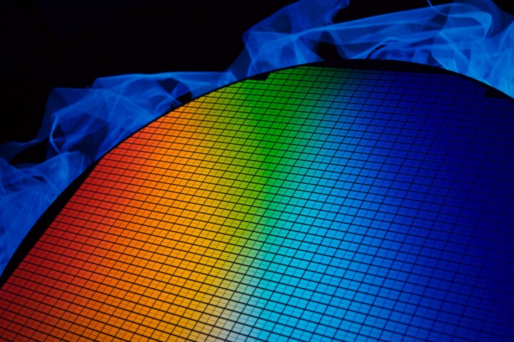
"Superatomic" material beats silicon for fastest semiconductor ever
October 31, 2023Scientists have found that a “superatomic” material is the fastest and most efficient semiconductor ever. Taking advantage of a tortoise-and-hare mechanism, the new material can transport energy much faster than silicon. -

Colorpik Pen draws from its surroundings to draw in 16 million colors
August 29, 2023With regular felt pens, users are limited to the colors of the pens in a set. As you might have guessed, though, the Colorpik Pen is different – it can reproduce 16 million colors, which are scanned from the user's environment. -

Portal, PlayStation’s first dedicated remote player, to launch late 2023
August 24, 2023Sony gave us a sneak peek of PlayStation’s first dedicated Remote Play device, then called Project Q, back in May. It's now provided more details and announced that the device, renamed Portal, will launch later this year. -

Plant-based PCB substrate breaks down in water for easier recycling
August 01, 2023Looking to tackle a significant part of our huge e-waste problem, Jiva has developed a PCB substrate that breaks down in water for easier recovery of materials. The startup is now partnering with manufacturers to demo and evaluate the Soluboards. -
Wireless charging technique boosts long-distance efficiency to 80%
July 24, 2023Adoption of wireless charging has been fairly slow, but it could pick up if it worked over longer distances. Now Aalto University engineers have developed a new system that can allow more efficient wireless power transmission over longer distances. -

Sol Reader puts bookworms right inside their ebooks
July 04, 2023If you're a really avid reader, you may resent the visual distractions that keep you from becoming thoroughly immersed in a book. That's where the Sol Reader comes in, as it fills your vision with text. -

Magmo Pro clings to iPhones, to auto-record phone calls
July 04, 2023While the iPhone can do many things, it doesn't perform what would seem like a relatively simple task – recording phone conversations. The Magmo Pro lets iPhone users do so, without going through any complicated procedures. -

Computer memory prototype ditches 1s and 0s for denser data storage
June 25, 2023Cambridge scientists have developed a new prototype for computer memory that could make for faster chips that could hold up to 100 times more data. The system is made up of barium bridges between films of a disordered material. -

Retro-cool Fineday 3.0 Bluetooth keyboard brings back the clickety-clack
May 26, 2023Although electric typewriters have been made almost entirely obsolete, there's something to be said for the satisfying "clickety-clack" of their keys. Well, that sound and feel is back, in the all-aluminum Fineday 3.0 Bluetooth Mechanical Keyboard. -

Nuwa Pen converts text written on regular paper into digital format
May 10, 2023For many people, taking notes using a pen and paper will always be easier and more intuitive than typing. The Nuwa Pen allows them to keep doing so, but it also digitizes what they've written for subsequent sharing and searchability. -
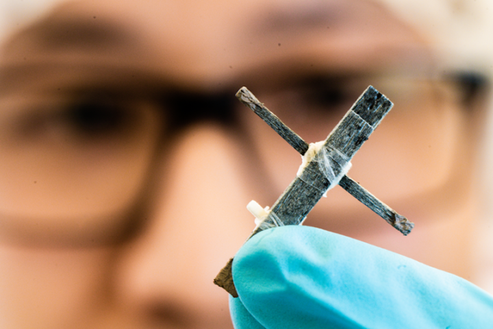
First working wooden transistor marks a step toward biodegradable tech
May 01, 2023Wood isn’t usually very good at conducting electricity, but now scientists have created the first functional wooden transistor. It’s not the best, and it requires some processing, but it does work and could help make for biodegradable electronics. -

Spore-producing bacteria battery could last 100 years on the shelf
April 18, 2023Researchers have developed a tiny battery that could be stored up to 100 years before being activated. The secret lies in sealing up dormant bacteria until it's time for them to be called into power-generating service.
Load More