Remarkable People
Technology has shaped our world in a countless ways. Here we celebrate the people who develop, distribute and push those technologies to unprecedented limits.
-

Lanny Smoot: First Disney Imagineer inducted into Inventors Hall of Fame
January 21, 2024With more than 100 patents, illustrious inventor Lanny Smoot is making history as the first Disney Imagineer to be inducted into the National Engineers Hall of Fame. The only other employee from The Walt Disney Company to do so is Walt Disney himself. -

High-tech entrepreneur Brett Adcock on Figure, Archer, and early success
October 02, 2023Brett Adcock has co-founded two companies on the bleeding edges of innovation in emerging markets: Archer Aviation, in the world of eVTOL aircraft, and Figure, in humanoid robots. We look into his background, and the startup that launched it all. -
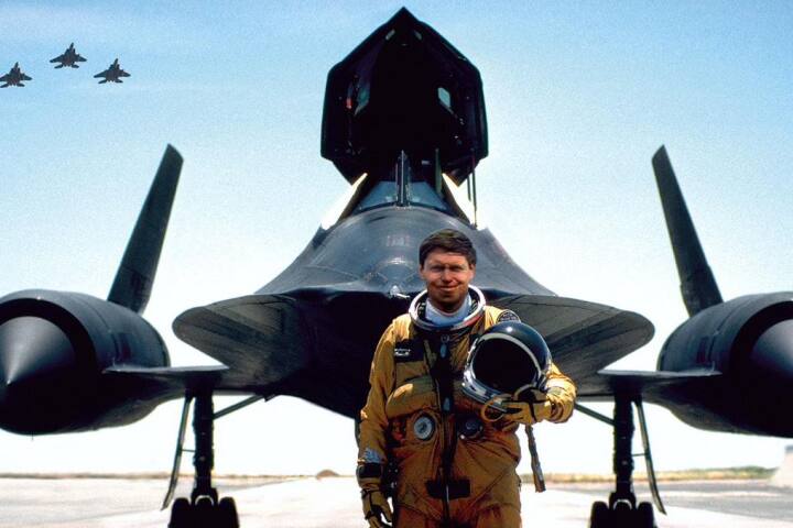
SR-71 pilot, photographer and storyteller Brian Shul dies at 75
May 21, 2023The aviation world has lost one of its brightest luminaries. Major Brian Shul was an incredible survivor and a top gun pilot – but also a gifted photographer and storyteller, whose stories about the extraordinary SR-71 Blackbird will live forever. -

Soggy professor breaks underwater-living record in sea habitat
May 16, 2023An adventurous professor from the University of South Florida has broken the world record for living in an underwater habitat. Joseph Dituri has called the submurged Jules’ Undersea Lodge home since March 1, and intends to remain there until June 9. -

Sir Ernest Shackleton's Endurance found after 107 years under the ice
March 09, 2022The wreck of one of the most famous exploration ships in history has been located. Using a robotic submersible, the Falklands Maritime Heritage Trust has found Sir Ernest Shackleton's Endurance, which was crushed in the Antarctic pack ice in 1915. -

Interview: Rocket-bike pilot Eddie Braun on his new Stuntman film
July 25, 2021New Atlas was at Snake River Canyon five years ago when Eddie Braun spectacularly finished the terrifying rocket bike jump that nearly killed Evel Knievel. The event is now a gorgeous documentary on Disney+, and we sat down with Braun to reminisce. -

Big, bold and beautiful: The incredible art of Christo and Jeanne-Claude
June 03, 2020The artist Christo recently passed away at the age of 84. For decades, he and his wife Jeanne-Claude made headlines with their striking and provocative artworks, such as installing a giant orange curtain between two mountain slopes in Colorado. -

How the invention of cut and paste helped change software forever
February 21, 2020After the death of Larry Tesler this week, New Atlas takes a brief look back at the invention of those now-ubiquitous computer commands: cut, copy and paste. -

Beautiful microorganism illustrations celebrated in new book
January 08, 2020A new book celebrating the science illustrations of Ernst Haeckel has launched on Kickstarter. The book features numerous drawings of microorganisms by the German zoologist and naturalist who identified thousands of new species during his career. -

Why Tim Berners-Lee didn't invent the internet
November 29, 2019Whenever computer scientist Sir Tim Berners-Lee makes the headlines, a significant minority of outlets inevitably, and wholly incorrectly, refer to him as “the inventor of the internet.” Here’s why they’re wrong. -

The curious case of the house with no knocker
October 16, 2019What connects the America's Cup, a dinner in Egypt and a house with no knocker? The answer is a man called Robert, born 216 years ago today, and his ill-fated sail boat: a schooner by the name of Titania. -

Eric Brende: How much technology do we need for a good and happy life?
October 14, 2019The Amish would be better off without so many horses, says this "technoskeptic" MIT graduate, who has dedicated his career to examining the 360-degree effects of technology on human life and happiness.
Load More